400-9988-118

|
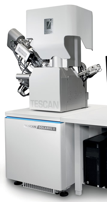
A Plasma FIB-SEM platform for deep sectioning and the highest resolution end-pointing for package level failure analysis • Curtaining-free large-area cross-sectioning for physical failure analysis of advanced packaging technologies • Prepare large area FIB-cross-sections up to 1 mm wide • Obtain low noise, high-resolution image at low keVs in short acquisition time at FIB-SEM coincidence with the sample tilted • Live SEM-monitoring during FIB milling for precise end-pointing • Observe the most beam-sensitive materials using low keVs ultra-high resolution for surface sensitivity and high material contrast • Effective techniques and recipes for fast and artefact-free cross-sectioning of composite samples (OLED and TFT displays, MEMS devices, isolation dielectrics) at high currents • Essence? easy-to-use modular user interface Complement TESCAN Solaris X capabilities with stand-alone laser ablation, which significantly improves time-to-result for large volume milling or access to deeply buried regions of interest, and frees the Plasma FIB for final targeted material removal, sample thinning or cross-section polishing. |
About Us|Honor|Products|Contact Us
Copyright ? 京ICP 06010381