400-9988-118

|
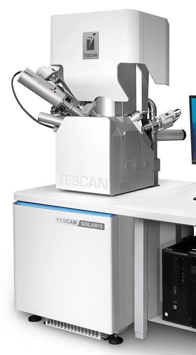
An alternative solution for semi-automated high-quality TEM lamella preparation • Low-kV ultra-high-resolution imaging of high-end semiconductor devices • Precise end-pointing at low electron beam energies • Gentle FIB thinning for improved quality results in TEM sample preparation enabled by excellent low-kV ion beam performance • Optimized workflows and recipes for easy preparation of ultra-thin TEM lamellae • Semi-automated software module for site-specific TEM lamella preparation • Preparation of advanced geometry TEM lamellae from the most advanced semiconductor nodes • Specialized, load-lock-compatible stage carousel for TEM sample preparation • Dedicated TEM grid holders with fully optimized geometry for advanced TEM sample preparation |
About Us|Honor|Products|Contact Us
Copyright ? 京ICP 06010381